")
")
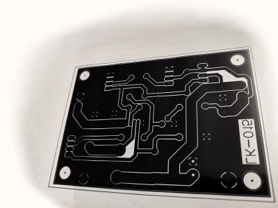
A big challenge in the practice of every radio amateur is undoubtedly the production of printed circuit boards. There are several methods that can be used. These include drawing a motif directly on the printed circuit board (PCB) with a marker, propisot sticks (now a rarity), or some kind of covering varnish, or the recently occurring production of PCBs by milling. Of course, there is also the possibility of ordering the production of a printed circuit board in a company that deals with the professional production of PCBs. Each of these methods has its own advantages and disadvantages. Probably still the most widespread method in radio amateur practice is the so called photo path method, which is also used in professional PCB production. With a little patience and acquired experience, it is possible to achieve high quality and an appearance similar to professional products with this method. One of the important components in this method of manufacturing printed circuit boards is the exposure unit. Its construction, for radio amateur needs, is described in this article.
General description of production technology
The basic principle of this procedure is the creation of the desired PCB motif by means of a photo-sensitive layer applied to the carrier material. The supporting material is usually an epoxy fiberglass board with a layer of copper on the surface. A pattern of the future printed circuit board, usually created on a computer and printed on a printer, but it can also be made by hand, is placed on a support material with a photo-sensitive layer (photoresist) applied to it and illuminated, usually with ultraviolet light, which causes the change properties of the photo-sensitive layer. This change causes the illuminated or non-illuminated portions of the photoresist to become soluble in the developer. By immersing the illuminated printed circuit board in the developer, the exposed or unexposed parts of the photoresist will be washed away, thereby exposing the surface layer of copper on the base material and allowing the exposed parts to be etched away, which will create the required conductive paths on the surface of the base material. Depending on whether the illuminated or non-illuminated parts of the photoresist are washed away in the developer, we speak of a positive or negative path, or of a positive or negative photoresist. The next step is to immerse the plate in an etching solution, which in amateur conditions is ferric chloride, or a mixture of hydrochloric acid and hydrogen peroxide, or sodium persulfate. After etching and removing the remaining photoresist, it is necessary to treat the board against oxidation, for which I use a solution of rosin in alcohol, which facilitates subsequent soldering of the components. ![]() The basic material of the printed circuit board can be purchased with already applied photoresist, or it is possible to apply the photoresist yourself. The advantage of buying DPS with a layer of photoresist already applied is that the layer of photoresist is homogeneous over the entire surface, has a defined thickness, and therefore the exposure is easier. The disadvantage is that when dividing the plates into smaller sizes, the photoresist may be scratched, which cannot be repaired at home, and in case of incorrect exposure, the plate cannot be used again. The use of photoresist in the POSITIV20 spray has proven successful for me. The main advantage is that I can use any base material, not only for printed circuit boards, and in case of any error, the process can be interrupted, the photo-sensitive layer can be washed off, a new layer can be applied and the whole process can be repeated.
The basic material of the printed circuit board can be purchased with already applied photoresist, or it is possible to apply the photoresist yourself. The advantage of buying DPS with a layer of photoresist already applied is that the layer of photoresist is homogeneous over the entire surface, has a defined thickness, and therefore the exposure is easier. The disadvantage is that when dividing the plates into smaller sizes, the photoresist may be scratched, which cannot be repaired at home, and in case of incorrect exposure, the plate cannot be used again. The use of photoresist in the POSITIV20 spray has proven successful for me. The main advantage is that I can use any base material, not only for printed circuit boards, and in case of any error, the process can be interrupted, the photo-sensitive layer can be washed off, a new layer can be applied and the whole process can be repeated.
PCB manufacturing process
As I said before, I use photosensitive spray varnish POSITIV20. I cut a piece of base material one centimeter larger than the required dimension of the printed circuit board, usually cuprextit class FR4, thickness 1.5 mm, but the choice of material depends on of the desired purpose. ![]() I use CITRA cleaning powder to clean the copper layer until it shines, thus the copper layer is free of mechanical impurities and grease, and the kitchen cleaning powder acts like fine emery, I dry the surface and, just to be sure, degrease it with a cloth soaked in alcohol. I spray a photo-sensitive layer on the DPS prepared in this way POZITIV20, which I dry at a temperature of 75 degrees within 15 minutes. If you have enough patience and time, you will place the board on the dark place and by the second day the layer will dry. I design printed circuit boards exclusively on the computer.
I use CITRA cleaning powder to clean the copper layer until it shines, thus the copper layer is free of mechanical impurities and grease, and the kitchen cleaning powder acts like fine emery, I dry the surface and, just to be sure, degrease it with a cloth soaked in alcohol. I spray a photo-sensitive layer on the DPS prepared in this way POZITIV20, which I dry at a temperature of 75 degrees within 15 minutes. If you have enough patience and time, you will place the board on the dark place and by the second day the layer will dry. I design printed circuit boards exclusively on the computer.  I will print the designed motif of the circuit board on a laser printer on a transparent foil in two copies, one copy mirror-inverted. I put these foils together with the printed layer so that the motif overlaps and put the foils into the laminating machine, where the applied toner acts as glue due to the temperature.
This step can be omitted if the contrast of the printed original is sufficient. I put the template prepared in this way together with the plate with the applied photoresist into the described exposure unit. Illumination with ultraviolet light in the described exposure unit lasts 3 minutes. I put the DPS illuminated in this way into the developer, which is a solution of sodium hydroxide (NaOH), prepared by dissolving 10 grams of solid NaOH in one liter of water. The illuminated parts of the photoresist are washed away within one to two minutes, after rinsing and visual inspection, etching in a solution of ferric chloride (FeCl3) follows. I drill the etched plate, remove the remaining photoresist with thinner C6000, or acetone and paint with a solution of dissolved rosin in thinner C6000..
Description, features and construction
The properties of the exposure unit have a significant impact on the final quality of the produced PCB. The basic properties of a good exposure unit include homogeneity of light over the entire exposure area, sufficient power and a good ability to ensure contact of the original with the surface of the circuit board. Discharge lamps are often used as a source of ultraviolet radiation. The use of discharge lamps has its pitfalls, primarily they need a higher excitation voltage, and I set myself the goal of making a device that would be easy to build. That was the reason why I decided to use UV LED strips. The wiring diagram of the lighting unit LK-016 is shown in the picture. .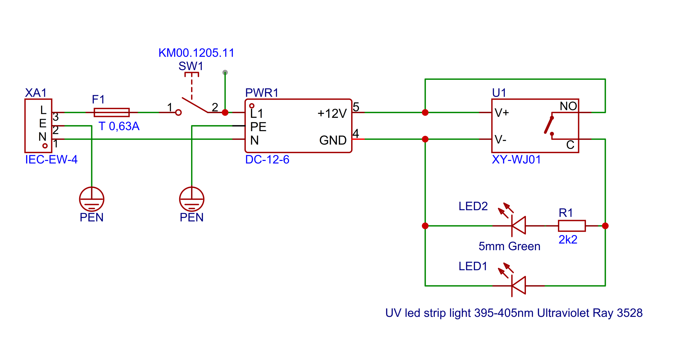 The entire electronics consists of several components, the basis of which are the already mentioned UV LED strips, which are placed on a self-adhesive mat 5 m long, marked as LED1 on the diagram. I used an LED strip made up of 120 SMD3528 diodes per one meter. One 5-meter strip is enough to cover a 17cm x 24.5cm light area homogeneously. Of course, it would be possible to use two 5-meter strips to increase the illumination area, but that did not seem reasonable to me, considering that for most amateur projects the size of the illumination area is 17 x 24.5 cm, and last but not least, the overall size of the device would also increase. The LED LED2, with a diameter of 5 mm, is powered through the resistor R1 and serves to signal the ongoing illumination when the unit cover is closed. The device is powered by a switched 12 volt source PWR1 with an output of 6 amperes. The exposure time can be set from a few seconds to a few hours using the U1 switching time unit type XY-WJ01 with display. As a tool box I used a medium-sized aluminum tool case with approximate dimensions of 39cm x 27cm x 14cm .
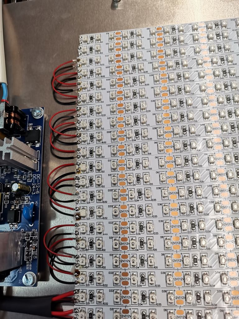
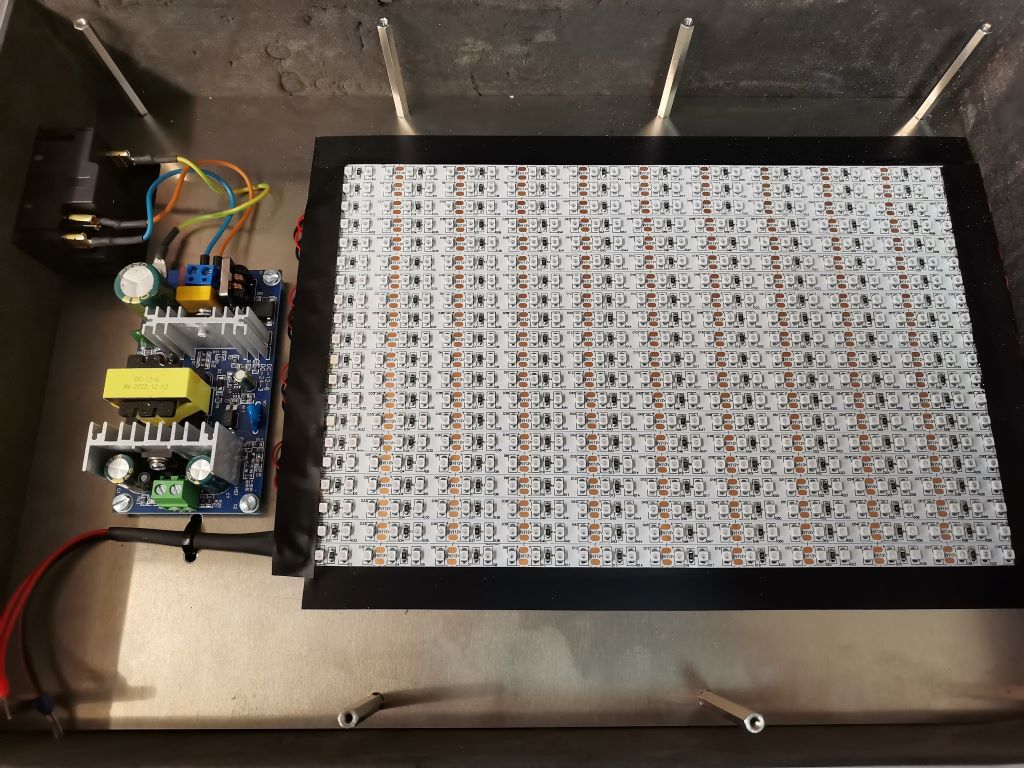 I mounted an aluminum panel with a thickness of 2 millimeters and dimensions of 36.7 cm x 24.7 cm to the bottom of the case on spacers 10 millimeters long. I glued LED strips cut to a length of approximately 25 cm containing 30 LEDs on the panel. I connected the first two LED strips to the PWR1 power supply and bridged the ends of these LED strips to adjacent ones with cables, so that a series-parallel connection of pairs of strips was created, as shown in the picture. The PWR1 power source is also attached to the panel. I cut a rectangular hole in the side wall of the case to hold the XA1 power connector. The body of the connector and XA1 also contains fuse F1 and switch SW1. The location of the panel at the bottom of the case, the supply connector and other elements is obvious from the next picture. Distance posts 5 cm long ensure the necessary distance between the bottom and top panels. I made the top panel from a 1 cm thick ABS electrician's mounting plate, into which I had a window of size 17 cm * 25 cm recessed 4 mm deep from the top surface, for mounting the milk glass, so that the top surface of the glass and the top surface of the panel were in one plane . I fixed the glass in the groove with transparent silicone sealant. I had the left part of the upper panel milled across the entire width to a depth of 5 millimeters so that the timer buttons are not under pressure when the lid is closed. I filled the cover with soft PUR foam to ensure the pressure of the template to the printed circuit board when the lid of the case is closed. This solution ensures an even pressure templates to the DPS pad, which minimizes backlighting.
 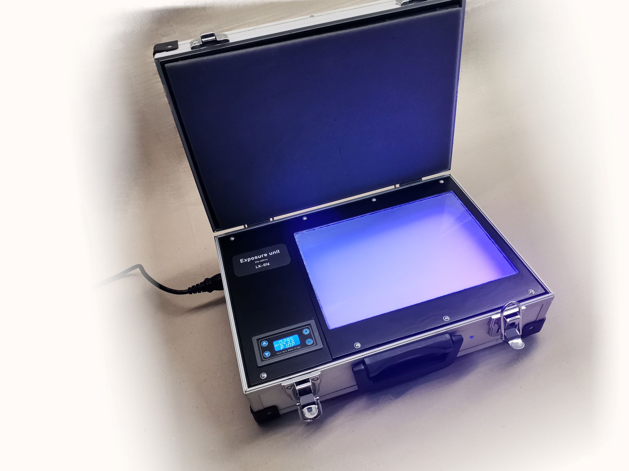 I placed the LED diode LED2 on the front panel of the case, so that the progress of illumination is signaled even when the lid of the case is closed. Working with the exposure unit is simple. Use the buttons to set the required time on the switching unit U1, in the case of using the photosensitive varnish POZITIV20 it is 180 seconds, place the template on the glass, place the PCB with the applied photosensitive layer on it, start the timer, close the lid and wait until LED2 goes out on the front panel of the case. signaling the ongoing enlightenment.
I would like to warn those interested in the construction that the bottom panel must be made of a good thermally conductive material, because a large number of ultraviolet LEDs generate heat, which the bottom panel absorbs and dissipates. Also, when choosing cover glass, care must be taken to ensure that it is well permeable to ultraviolet radiation, I used sandblasted glass because frosted glass is unavailable in such small quantities as I needed for my project.
Conclusion
This equipment will significantly improve the quality of production of prototype boards in every workshop. The simple construction and implementation is also suitable for beginners. All necessary files to implement this project are available in the section download.